-
Notifications
You must be signed in to change notification settings - Fork 21
Pano Data Block
The SPI flash block at address 0x000e0000 (G1), 0x8c0000 (G2 Rev B) or 0x6b0000 (G2_C) appears to be a data block which is programmed by the factory with device specific information.
The meaning of most of the data in this block is unknown.
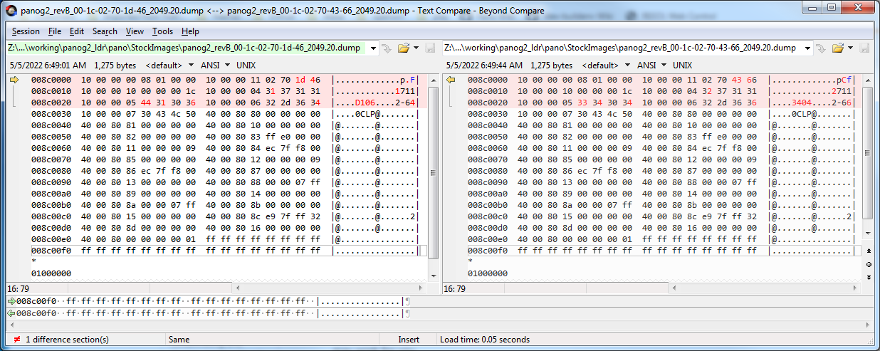
These are the differences between two G2 Rev B Panos that both programmed with revision 2049.20 of the bitstream.
The MAC address of the Pano on the left side is 00:1c:02:70:1d:46, the right is 00:1c:02:70:43:66 from the dump we can guess that the 4 bytes at offset 0x0c of the block are the last 4 bytes of the MAC address.
Please see the next section rather than relying on this offset based on observations of 2 random Panos.
Disassembly of prog_fpga by Ghirdra reveals that the Pano has "Configuration Registers" which are readable and writable via TNP. Based on some guess work plus known values such as the board ID reported by discovery and the MAC address we can make a guess of how the configuration data is stored in the data block.
| Byte | Usage | Notes |
|---|---|---|
| 0 | Flags | The only values observed are 0x10 and 0x40. It appears that 0x40 are the default values and 0x10 are values which have been set. |
| 1 | always 0 | unknown |
| 2 | 0x00 or 0x80 | unknown |
| 3 | Configuration register number | |
| 4 -> 7 | 32 bit Value |
| Register | Usage | Notes |
|---|---|---|
| 0x00 | Board ID | G1: 0x00050000 G2: 0x08010000 G2_C: 0x08010002 |
| 0x10 | Upper 2 bytes of MAC Adr | |
| 0x11 | Lower 4 bytes of MAC Adr |
