-
Notifications
You must be signed in to change notification settings - Fork 0
DPP2Lora

-
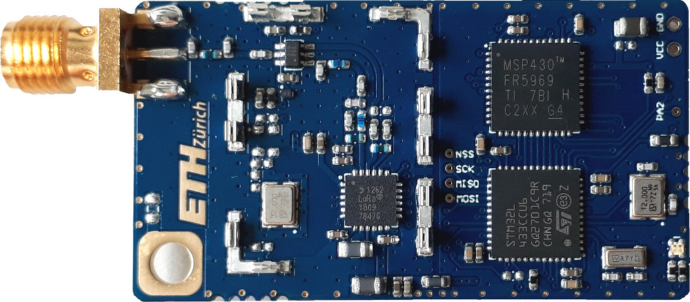
COM Processor: STM32L433CCU6 ARM Cortex M4 microcontroller (datasheet, ref. manual)
- Flash memory: 256 KB
-
Radio Chip: Semtech SX1262 868 MHz LoRa transceiver (datasheet)
- Tx Power: up to +22 dBm
- BOLT: TI MSP430FR5969 MCU (BOLT)
- RF shield
- COM processor oscillators:
- HFXT: 12 MHz
- LFXT: 32.768 kHz
- Radio oscillator:
- default: 32 MHz XT
- optional 32 MHz TCXO (not installed)
- Schematics (PCB design)
Note: In order to work with the DPP2LoRa COM board, it needs to be stacked onto an application board (e.g. the DevBoard. Stack the COM board onto the application board and fix it with appropriate hardware (spacer, screw, nut).
- A basic blink LED code example (bare metal) can be found in our repository.
- More code is available in the Flora repository.
We use the STM32CubeIDE software from to develop and compile code for the SX126x platform.
Compiled binary is located in the Debug directory of the project root after build.
objcopy -O ihex input.elf output.hex
There are 2 options:
- Note: A DPP DevBoard is required to connect a debugger to the SX126x COM board.
- Note: Only the SWD protocol is supported on the DevBoard. JTAG is not supported on the DPP2 DevBoard.
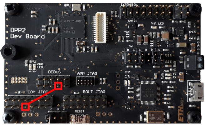
- Make sure that the small 10-pin COM JTAG connector (highlighted in red in the image below) is installed, solder it if necessary.

The jumpers on the DevBoard VCC header can either be as shown above or with an additional jumper at the marker 'B'.
-
Software: Programming with a debugger hardware is integrated into the STM32CubeIDE development IDE.
- In order to use the Segger J-Link for debugging, the target configuration needs to be adjusted. In STM32CubeIDE, go to project settings > C/C++ Build > Settings. Select the MCU (STM32L433CC) in the tab Target Settings and apply the changes. Then go to Run/Debug Settings and click edit. In the tab Debugger, make sure SWD is selected as interface (since JTAG is not supported on the DPP2 DevBoard).
-
Hardware: Programming is supported and tested with Segger J-Link debuggers:
- Segger J-Link EDU Mini debug emulator with a 10-pin ribbon cable
- Segger J-Link debug probe with an adapter from 20 to 10-pin.
- Note: A DPP DevBoard is required to connect the micro-USB cable to the COM board.
-
Hardware
- If you want to be able to program the MCU via USB (UART bootloader), then connect pin 7 of COM_JTAG and pin 7 of the DEBUG header with a jumper wire (as shown below).

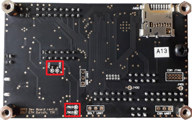
In addition, make sure that the solder jumpers J500, J501, J502 and J503 on the backside of the DevBoard are closed (see below).

- If you want to be able to program the MCU via USB (UART bootloader), then connect pin 7 of COM_JTAG and pin 7 of the DEBUG header with a jumper wire (as shown below).
-
Software
- Install the following python packages:
python3 -m pip install pyserial intelhex stm32loader - Get the STM32 programming script. The script runs on Linux, but may need some adjustment on a Windows machine.
- In order to flash a binary to the STM32L4 MCU on the DPP2LoRa COM board use the following command:
./program_stm32.py <path to .hex or .elf>
The script should automatically choose the right serial port. If you have more than one board connected, then you need to specify the serial port manually as a second argument.
- Install the following python packages:
DevBoard: Notice that when using this ComBoard together with the DPP DevBoard, BOLT_VCC (VCC Select Pin 6) and COM_VCC (VCC Select Pin 8) are connected on the ComBoard. Therefore, for power measurements of the ComBoard, both jumpers (C and B) must be disconnected.
FlockLab: The boards that are available as targets on FlockLab (DPP2LoRa and DPP2LoRaHG) have the resistor R200 (see schematic) placed with a 220 Ohm part (measured on a single board). Therefore, it is essential that Pin PB.3 (COM_GPIO2) is not left floating, as this can lead to significant observable leakage currents up to 50mA. Similarly, Pin PH.3 (COM_GPIO1) should not be used and always remain cleared, as FlockLab is actively driving it low because it is connected to TARGETx_PROG.
| GPIO | Name | Mapping/Function on DevBoard | Mapping/Function on FlockLab |
|---|---|---|---|
| PA0 | COM_IND | BOLT indication line (input) | FLOCKLAB_SIG1 (actuation input) |
| PA3 | COM_TREQ | BOLT time request (input) | FLOCKLAB_INT1 (tracing output) |
| PA4 | APP_IND | BOLT output queue indication line (input) | FLOCKLAB_SIG2 (actuation input) |
| PA9 | COM_TXD | Serial logging and BSL programming (input) | Serial logging and BSL programming |
| PA10 | COM_RXD | Serial logging and BSL programming (output) | Serial logging and BSL programming |
| PA13 | COM_PROG2 | Pin #9 on debug header (input or output) | FLOCKLAB_LED3 (tracing output) |
| PA14 | COM_PROG | SWCLK (target programming via SWD) | FLOCKLAB_LED1 (tracing output) |
| PA15 | RFDIO1 | n/a | FLOCKLAB_LED2 (tracing output) |
| PB3 | COM_GPIO2 | Pin #8 on debug header (input or output) | FLOCKLAB_LED2 (tracing output) |
| PH3 | COM_GPIO1 | Pin #7 on debug header (input or output) | BSL entry pin |
| GPIO | Assigned name, function | Recommended config |
|---|---|---|
| PA0 | COM_IND, BOLT input queue indicator | Input |
| PA1 | Unused | Analog |
| PA2 | Unused (test point) | Analog |
| PA3 | COM_TREQ, BOLT time request line | Input with pulldown |
| PA4 | APP_IND, BOLT output queue indicator | Input |
| PA5 | COM_SCK, BOLT SPI serial clock | Module function (on FlockLab: output low) |
| PA6 | COM_MISO, BOLT SPI master input | Module function (on FlockLab: output low) |
| PA7 | COM_MOSI, BOLT SPI master output | Module function (on FlockLab: output low) |
| PA8 | RF_RST, SX1262 radio reset line | |
| PA9 | COM_TXD, UART transmit | Module function |
| PA10 | COM_RXD, UART receive | Module function |
| PA11 | RF_BUSY, SX1262 radio busy indicator | Input |
| PA12 | RF_SW, SX1262 antenna switch on/off | Output |
| PA13 | COM_PROG2, GPIO pin or SWDIO | - |
| PA14 | COM_PROG, SWCLK | - |
| PA15 | RF_DIO1, SX1262 radio DIO1 pin | Input |
| PB0 | COM_ACK, BOLT acknowledgement line | Input (on FlockLab: with pulldown) |
| PB1 | COM_REQ, BOLT request line | Output low |
| PB2 | COM_MODE, BOLT mode select | Output |
| PB3 | COM_GPIO2, GPIO pin or SWO | on Flocklab: Input! |
| PB4 | Unused | Analog |
| PB5 | Unused | Analog |
| PB6 | Unused | Analog |
| PB7 | Unused | Analog |
| PB8 | COM_LED2, LED | Output |
| PB9 | COM_LED1, LED | Output |
| PB10 | Unused | Analog |
| PB11 | Unused | Analog |
| PB12 | RF_NSS, SX1262 radio SPI slave select | Module function or output |
| PB13 | RF_SCK, SX1262 radio SPI serial clock | Module function |
| PB14 | RF_MISO, SX1262 radio SPI master input | Module function |
| PB15 | RF_MOSI, SX1262 radio SPI master output | Module function |
| PC13 | Connected to PA15 | Input |
| PC14 | LFXT_IN, 32kHz crystal oscillator | OSC32_IN |
| PC15 | LFXT_OUT, 32kHz crystal oscillator | OSC32_OUT |
| PH0 | HFXT_IN, 12MHz crystal oscillator | OSC_IN |
| PH1 | HFXT_IN, 12MHz crystal oscillator | OSC_OUT |
| PH3 | COM_GPIO1, GPIO pin or BOOT0 | - |
| NRST | COM_RST, MCU reset | - |
In order to program the LoRa ComBoard on the Baseboard, a minor hardware patch is required. Connect the pins 18 and 22 of the board-to-board connector with a resistor (~1k ohm):

Before installing a DPP2 LoRa comboard on a FlockLab observer, the following patch needs to be applied:
- make sure the resistor R200 is removed
- connect PA15 with COM_GPIO1 via a 220 ohm resistor. You can do that by using a 0603 sized resistor and placing it such that one pad of R200 is connected with one pad of R201 as shown in the photo below.

- For the use together with a DevBoard: see DPP SerialOutput info.